- 您现在的位置:买卖IC网 > Sheet目录368 > UPD44646363AF5-E22-FQ1-A (Renesas Electronics America)SRAM DDRII 72MBIT 165-PBGA
�� �
�
�μ� PD44646092A-A,� 44646182A-A,� 44646362A-A,� 44646093A-A,� 44646183A-A,� 44646363A-A�
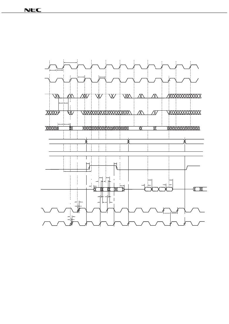
�Read� and� Write� Timing�
�2.0� Clock� Cycles� Read� Latency�
�[� μ� PD44646092A-A],� [� μ� PD44646182A-A],� [� μ� PD44646362A-A]�
�NOP�
�READ�
�READ�
�NOP�
�NOP�
�NOP�
�WRITE�
�WRITE�
�READ�
�(burst� of� 2)� (burst� of� 2)�
�(burst� of� 2)� (burst� of� 2)� (burst� of� 2)�
�1�
�2�
�3�
�4�
�5�
�6�
�7�
�8�
�9�
�10�
�11�
�TKHKH�
�K�
�K#�
�LD#�
�R,� W#�
�TKHKL� TKLKH�
�TIVK� H�
�T� KHIX�
�TKHK#H�
�TK#HKH�
�TAVKH�
�TKHAX�
�Address�
�ODT� state�
�DQ�
�A0�
�ODT-ON�
�A1�
�ODT-OFF�
�A2�
�A3�
�A4�
�ODT-ON�
�ODT-OFF�
�ODT� state�
�BW#�
�QVLD�
�TCQHQVLD�
�Read� Latency� =� 2.0� clock� cycles�
�ODT-ON�
�TCQHQVLD�
�TKHQV�
�T� KHQV�
�TKHDX�
�TKHDX�
�TKHQ� X�
�T� KHQX�
�TKHQZ�
�TDVKH�
�TDVKH�
�TKHCQX1�
�DQ�
�Q00�
�Q01�
�Q10�
�Q11�
�D20�
�D21�
�D30�
�D31�
�Q40�
�Q41�
�TCQHQX�
�TCQHQX�
�CQ�
�TKHCQV�
�TKHCQX�
�TKHCQV�
�TCQHQV�
�TCQHQ� V�
�TCQHCQ#H� T� CQ#HCQH�
�TKHCQX�
�CQ#�
�Remarks� 1.� Q00� refers� to� output� from� address� A0.�
�Q01� refers� to� output� from� the� next� internal� burst� address� following� A0,� etc.�
�2.� Outputs� are� disabled� (high� impedance)� 3� clock� cycles� after� the� last� READ� (LD#� =� LOW,� R,� W#� =� HIGH)�
�is� input� in� the� sequences� of� [READ]-[NOP].�
�3.� The� third� NOP� cycle� between� Read� to� Write� transition� may� not� be� necessary� for� correct� device�
�operation� when� Read� latency� =� 2.0� clock� cycles.� However,� it� may� be� required� to� avoid� bus� contention.�
�4.� When� the� ODT� control� pin� is� LOW� or� No� Connect,� the� ODT� function� is� always� off.�
�20�
�Data� Sheet� M19960EJ2V0DS�
�发布紧急采购,3分钟左右您将得到回复。
相关PDF资料
UPD44647366AF5-E22-FQ1-A
SRAM QDRII 72MBIT 165-PBGA
USB-100
KIT STARTER FOR USB
USBMLCF
USB BDM INTERFACE MC P&E
USBMLPPCBDM
MULTILINK P&E POWERPC USB
V-9767-L
DOOR ECONOGLAS 19" LOCKING
VC-9931
CABINT VISNCB 20.54X23.62X23.62"
VC-9934B
VISIONCAB B 35.40X23.62X23.62"
VLA500-01
IC IGBT GATE DVR/DC-DC CONV 12A
相关代理商/技术参数
UPD44646363AF5-E25-FQ1
功能描述:SRAM DDRII 72MBIT 165-PBGA RoHS:是 类别:集成电路 (IC) >> 存储器 系列:- 标准包装:3,000 系列:- 格式 - 存储器:EEPROMs - 串行 存储器类型:EEPROM 存储容量:8K (1K x 8) 速度:400kHz 接口:I²C,2 线串口 电源电压:1.7 V ~ 5.5 V 工作温度:-40°C ~ 85°C 封装/外壳:8-SOIC(0.154",3.90mm 宽) 供应商设备封装:8-SOIC 包装:带卷 (TR)
UPD44646363AF5-E25-FQ1-A
功能描述:SRAM DDRII 72MBIT 165-PBGA RoHS:是 类别:集成电路 (IC) >> 存储器 系列:- 标准包装:3,000 系列:- 格式 - 存储器:EEPROMs - 串行 存储器类型:EEPROM 存储容量:8K (1K x 8) 速度:400kHz 接口:I²C,2 线串口 电源电压:1.7 V ~ 5.5 V 工作温度:-40°C ~ 85°C 封装/外壳:8-SOIC(0.154",3.90mm 宽) 供应商设备封装:8-SOIC 包装:带卷 (TR)
UPD44647186AF5-E22-FQ1
功能描述:SRAM QDRII 72MBIT 165-PBGA RoHS:是 类别:集成电路 (IC) >> 存储器 系列:- 标准包装:1,000 系列:- 格式 - 存储器:RAM 存储器类型:SRAM - 双端口,同步 存储容量:1.125M(32K x 36) 速度:5ns 接口:并联 电源电压:3.15 V ~ 3.45 V 工作温度:-40°C ~ 85°C 封装/外壳:256-LBGA 供应商设备封装:256-CABGA(17x17) 包装:带卷 (TR) 其它名称:70V3579S5BCI8
UPD44647186AF5-E22-FQ1-A
功能描述:SRAM QDRII 72MBIT 165-PBGA RoHS:是 类别:集成电路 (IC) >> 存储器 系列:- 标准包装:3,000 系列:- 格式 - 存储器:EEPROMs - 串行 存储器类型:EEPROM 存储容量:8K (1K x 8) 速度:400kHz 接口:I²C,2 线串口 电源电压:1.7 V ~ 5.5 V 工作温度:-40°C ~ 85°C 封装/外壳:8-SOIC(0.154",3.90mm 宽) 供应商设备封装:8-SOIC 包装:带卷 (TR)
UPD44647186AF5-E25-FQ1
功能描述:SRAM QDRII 72MBIT 165-PBGA RoHS:是 类别:集成电路 (IC) >> 存储器 系列:- 标准包装:3,000 系列:- 格式 - 存储器:EEPROMs - 串行 存储器类型:EEPROM 存储容量:8K (1K x 8) 速度:400kHz 接口:I²C,2 线串口 电源电压:1.7 V ~ 5.5 V 工作温度:-40°C ~ 85°C 封装/外壳:8-SOIC(0.154",3.90mm 宽) 供应商设备封装:8-SOIC 包装:带卷 (TR)
UPD44647186AF5-E25-FQ1-A
功能描述:SRAM QDRII 72MBIT 165-PBGA RoHS:是 类别:集成电路 (IC) >> 存储器 系列:- 标准包装:3,000 系列:- 格式 - 存储器:EEPROMs - 串行 存储器类型:EEPROM 存储容量:8K (1K x 8) 速度:400kHz 接口:I²C,2 线串口 电源电压:1.7 V ~ 5.5 V 工作温度:-40°C ~ 85°C 封装/外壳:8-SOIC(0.154",3.90mm 宽) 供应商设备封装:8-SOIC 包装:带卷 (TR)
UPD44647366AF5-E22-FQ1
功能描述:SRAM QDRII 72MBIT 165-PBGA RoHS:是 类别:集成电路 (IC) >> 存储器 系列:- 标准包装:3,000 系列:- 格式 - 存储器:EEPROMs - 串行 存储器类型:EEPROM 存储容量:8K (1K x 8) 速度:400kHz 接口:I²C,2 线串口 电源电压:1.7 V ~ 5.5 V 工作温度:-40°C ~ 85°C 封装/外壳:8-SOIC(0.154",3.90mm 宽) 供应商设备封装:8-SOIC 包装:带卷 (TR)
UPD44647366AF5-E22-FQ1-A
功能描述:SRAM QDRII 72MBIT 165-PBGA RoHS:是 类别:集成电路 (IC) >> 存储器 系列:- 标准包装:3,000 系列:- 格式 - 存储器:EEPROMs - 串行 存储器类型:EEPROM 存储容量:8K (1K x 8) 速度:400kHz 接口:I²C,2 线串口 电源电压:1.7 V ~ 5.5 V 工作温度:-40°C ~ 85°C 封装/外壳:8-SOIC(0.154",3.90mm 宽) 供应商设备封装:8-SOIC 包装:带卷 (TR)